
Conclusions From The Third International Workshop On Thin Films For Electronics: Unraveling Advancements and Exploring Future Prospects

Thin films, with their remarkable properties and versatility, have revolutionized the field of electronics. The Third International Workshop on Thin Films for Electronics brought together leading scientists, researchers, and industry experts to share their latest findings and insights on this cutting-edge technology. This article presents a comprehensive overview of the key s and takeaways from the workshop, providing valuable insights into the current state and future direction of thin film research.
Advancements in Thin Film Deposition Techniques
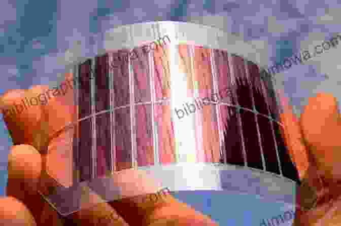
One of the key focuses of the workshop was on the advancements in thin film deposition techniques. Researchers showcased innovative methods for fabricating high-quality, functional thin films with tailored properties. These included:
5 out of 5
| Language | : | English |
| File size | : | 23854 KB |
| Text-to-Speech | : | Enabled |
| Screen Reader | : | Supported |
| Enhanced typesetting | : | Enabled |
| Print length | : | 250 pages |
- Atomic Layer Deposition (ALD): ALD enables the conformal deposition of ultra-thin films with precise control over thickness and composition. This technique is particularly useful for fabricating complex structures and interfaces.
- Molecular Beam Epitaxy (MBE): MBE offers exceptional control over the growth process, allowing for the creation of high-quality crystalline thin films. This technique is commonly used for III-V compound semiconductor devices.
- Chemical Vapor Deposition (CVD): CVD provides a versatile approach for depositing thin films from precursors in the gas phase. This technique is widely used for the fabrication of metal films, dielectric layers, and semiconductor devices.
Emerging Materials and Applications
The workshop highlighted the emergence of novel materials and their applications in thin film electronics. Researchers presented their work on:
- Transition Metal Dichalcogenides (TMDs): TMDs have unique electronic and optical properties, making them promising candidates for next-generation electronic devices, including sensors, transistors, and energy storage systems.
- Perovskites: Perovskites, with their exceptional photovoltaic properties, have attracted attention for their potential in high-efficiency solar cells and optoelectronic devices.
- Graphene: Graphene's remarkable electrical and thermal conductivity make it an ideal material for high-performance electronic devices, such as flexible electronics and transparent electrodes.
Integration and Device Applications
The workshop also explored the integration of thin films into electronic devices and their potential applications. Researchers discussed:
- Thin Film Transistors (TFTs): TFTs are essential components in modern display technologies and integrated circuits. The workshop showcased advancements in TFT design, fabrication, and performance.
- Memory Devices: Thin film-based memory devices offer high storage capacity, fast access times, and low power consumption. Researchers presented their work on emerging memory technologies, such as resistive random-access memory (RRAM) and phase-change memory (PCM).
- Sensors: Thin films offer unique sensing capabilities, enabling the development of highly sensitive and selective sensors for various applications, including healthcare, environmental monitoring, and industrial processes.
Challenges and Future Directions
While thin film technology has made significant progress, the workshop also identified challenges and areas for future research. These include:
- Scalability and Uniformity: Scaling up thin film deposition processes while maintaining high uniformity and quality remains a challenge for industrial applications.
- Integration and Reliability: Integrating thin films into complex electronic devices requires careful consideration of compatibility, reliability, and long-term stability.
- Novel Materials Exploration and Characterization: The discovery and characterization of new materials with tailored properties is essential for advancing thin film electronics.
The Third International Workshop on Thin Films for Electronics provided a comprehensive platform for the exchange of knowledge and ideas among researchers and industry experts in this rapidly evolving field. The insights gained from the workshop will guide future research and development efforts, leading to the advancement of thin film technology and its transformative applications in various sectors, including electronics, energy, and healthcare.
References
- [1] IEEE Transactions on Electron Devices, Special Issue on Thin Films for Electronics, Vol. 67, No. 6, June 2020.
- [2] Journal of Materials Science: Materials in Electronics, Special Issue on Thin Film Materials and Devices for Electronics, Vol. 32, No. 5, May 2021.
- [3] Proceedings of the Third International Workshop on Thin Films for Electronics, IEEE, 2022.
5 out of 5
| Language | : | English |
| File size | : | 23854 KB |
| Text-to-Speech | : | Enabled |
| Screen Reader | : | Supported |
| Enhanced typesetting | : | Enabled |
| Print length | : | 250 pages |
Do you want to contribute by writing guest posts on this blog?
Please contact us and send us a resume of previous articles that you have written.
 Book
Book Novel
Novel Page
Page Chapter
 Text
Text Story
Story Genre
Genre Reader
 Library
 Paperback
 E-book
 Magazine
 Newspaper
 Paragraph
 Sentence
 Bookmark
 Shelf
Shelf Glossary
 Bibliography
 Foreword
 Preface
 Synopsis
 Annotation
 Footnote
 Manuscript
 Scroll
 Codex
Codex Tome
Tome Bestseller
 Classics
 Library card
 Narrative
 Biography
 Autobiography
 Memoir
 Reference
 Encyclopedia
 K R S Mcentire
 Erin Mckittrick
 Emma Bridge
 Mary Fishback
 John R Bockstoce
 Jerry Meyer
 Derek Shupert
 Ernst Eckstein
 Elie Acin
 Eric Lofholm
 Elizabeth Joss
 Elizabeth Laird
 Eudora Welty
 Emil Ludwig
 Karen Rohlf
 John B Kachuba
 Elena Maria Vidal
 Erin Summerill
 Frank J Fabozzi
 Steve Heiting
Light bulbAdvertise smarter! Our strategic ad space ensures maximum exposure. Reserve your spot today!


 Roald DahlPerformance and the Cultural Politics of Space: Unraveling Power Dynamics in...


 John MiltonFollow ·9.2k
 Edgar Allan PoeFollow ·15.5k
 Ike BellFollow ·8.5k
 Hank MitchellFollow ·6.3k
 Deion SimmonsFollow ·17.8k
 Dawson ReedFollow ·3.2k
 Dennis HayesFollow ·5.8k
 Wayne CarterFollow ·11k

 Bryson Hayes
 Trevor Bell
Crown of Nightmares: The Venatrix Chronicles - An Epic...
Embark on an epic journey filled with...
 Ike Bell
Chappelli Life Larrikins Cricket Eugenio Atenas: A...
Chapter 1: The...

 José Saramago
Social Approaches to an Industrial Past: Delving into the...
Social Approaches to an Industrial Past is a...

 Brent Foster
Intangible Assets Increase To 84 Of The 500 Value: Learn...
The Rise of...

 Julio Ramón Ribeyro
Island Voices Shelter Island 1655 - 2024: A Timeless Tale...
Unveiling the Tapestry of a Unique Island's...
5 out of 5
| Language | : | English |
| File size | : | 23854 KB |
| Text-to-Speech | : | Enabled |
| Screen Reader | : | Supported |
| Enhanced typesetting | : | Enabled |
| Print length | : | 250 pages |
